A100


- Manufacturer :
- NVIDIA
- Product Category :
- Miscellaneous
- Datasheets
- A100
The A100 GPU includes a revolutionary new multi-instance GPU (MIG) virtualization and GPU partitioning capability that is particularly beneficial to cloud service providers (CSPs). When configured for MIG operation, the A100 permits CSPs to improve the utilization rates of their GPU servers, delivering up to 7x more GPU Instances for no additional cost. Robust fault isolation allows them to partition a single A100 GPU safely and securely.
A100 adds a powerful new third-generation Tensor Core that boosts throughput over V100 while adding comprehensive support for DL and HPC data types, together with a new Sparsity feature that delivers a further doubling of throughput.
New TensorFloat-32 (TF32) Tensor Core operations in A100 provide an easy path to accelerate FP32 input/output data in DL frameworks and HPC, running 10x faster than V100 FP32 FMA operations or 20x faster with sparsity. For FP16/FP32 mixed-precision DL, the A100 Tensor Core delivers 2.5x the performance of V100, increasing to 5x with sparsity.
New Bfloat16 (BF16)/FP32 mixed-precision Tensor Core operations run at the same rate as FP16/FP32 mixed-precision. Tensor Core acceleration of INT8, INT4, and binary round out support for DL inferencing, with A100 sparse INT8 running 20x faster than V100 INT8. For HPC, the A100 Tensor Core includes new IEEE-compliant FP64 processing that delivers 2.5x the FP64 performance of V100.
The NVIDIA A100 GPU is architected to not only accelerate large complex workloads, but also efficiently accelerate many smaller workloads. A100 enables building data centers that can accommodate unpredictable workload demand, while providing fine-grained workload provisioning, higher GPU utilization, and improved TCO.
The NVIDIA A100 GPU delivers exceptional speedups over V100 for AI training and inference workloads as shown in Figure 2. Similarly, Figure 3 shows substantial performance improvements across different HPC applications.
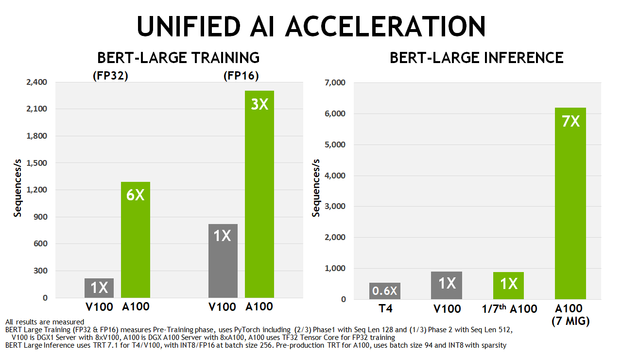 Figure 2. A100 GPU performance in BERT deep learning training and inference scenarios compared to NVIDIA Tesla V100 and NVIDIA Tesla T4.
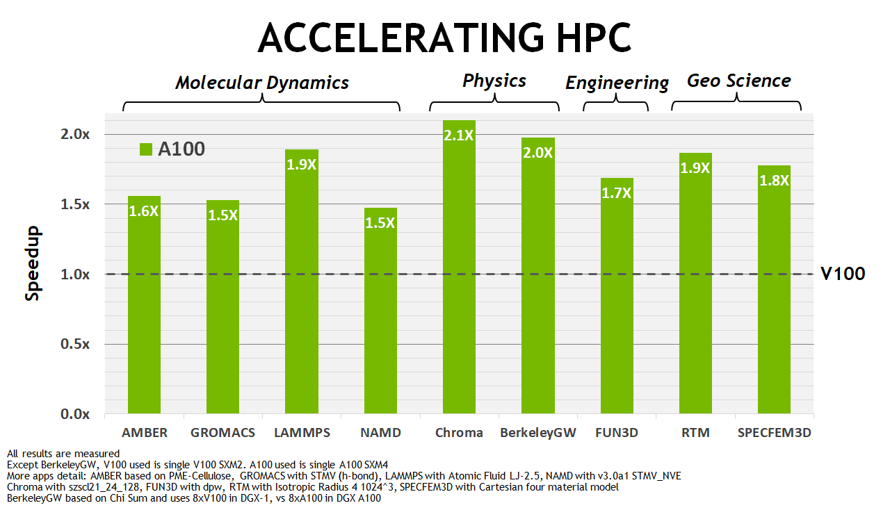 Figure 3. A100 GPU HPC application speedups compared to NVIDIA Tesla V100.
Key features
Fabricated on the TSMC 7nm N7 manufacturing process, the NVIDIA Ampere architecture-based GA100 GPU that powers A100 includes 54.2 billion transistors with a die size of 826 mm2.
A100 GPU streaming multiprocessor
The new streaming multiprocessor (SM) in the NVIDIA Ampere architecture-based A100 Tensor Core GPU significantly increases performance, builds upon features introduced in both the Volta and Turing SM architectures, and adds many new capabilities.
The A100 third-generation Tensor Cores enhance operand sharing and improve efficiency, and add powerful new data types, including the following:
TF32 Tensor Core instructions that accelerate processing of FP32 data
IEEE-compliant FP64 Tensor Core instructions for HPC
BF16 Tensor Core instructions at the same throughput as FP16
| Peak FP641 | 9.7 TFLOPS |
| Peak FP64 Tensor Core1 | 19.5 TFLOPS |
| Peak FP321 | 19.5 TFLOPS |
| Peak FP161 | 78 TFLOPS |
| Peak BF161 | 39 TFLOPS |
| Peak TF32 Tensor Core1 | 156 TFLOPS | 312 TFLOPS2 |
| Peak FP16 Tensor Core1 | 312 TFLOPS | 624 TFLOPS2 |
| Peak BF16 Tensor Core1 | 312 TFLOPS | 624 TFLOPS2 |
| Peak INT8 Tensor Core1 | 624 TOPS | 1,248 TOPS2 |
| Peak INT4 Tensor Core1 | 1,248 TOPS | 2,496 TOPS2 |
Table 1. A100 Tensor Core GPU performance specs.
1) Peak rates are based on the GPU boost clock.
2) Effective TFLOPS / TOPS using the new Sparsity feature.
New Sparsity support in A100 Tensor Cores can exploit fine-grained structured sparsity in DL networks to double the throughput of Tensor Core operations. Sparsity features are described in detail in the A100 introduces fine-grained structured Sparsity section later in this post.
The larger and faster L1 cache and shared memory unit in A100 provides 1.5x the aggregate capacity per SM compared to V100 (192 KB vs. 128 KB per SM) to deliver additional acceleration for many HPC and AI workloads.
Several other new SM features improve efficiency and programmability and reduce software complexity.
40 GB HBM2 and 40 MB L2 cache
To feed its massive computational throughput, the NVIDIA A100 GPU has 40 GB of high-speed HBM2 memory with a class-leading 1555 GB/sec of memory bandwidth—a 73% increase compared to Tesla V100. In addition, the A100 GPU has significantly more on-chip memory including a 40 MB Level 2 (L2) cache—nearly 7x larger than V100—to maximize compute performance. With a new partitioned crossbar structure, the A100 L2 cache provides 2.3x the L2 cache read bandwidth of V100.
To optimize capacity utilization, the NVIDIA Ampere architecture provides L2 cache residency controls for you to manage data to keep or evict from the cache. A100 also adds Compute Data Compression to deliver up to an additional 4x improvement in DRAM bandwidth and L2 bandwidth, and up to 2x improvement in L2 capacity.
Multi-Instance GPU
The new Multi-Instance GPU (MIG) feature allows the A100 Tensor Core GPU to be securely partitioned into as many as seven separate GPU Instances for CUDA applications, providing multiple users with separate GPU resources to accelerate their applications.
With MIG, each instance’s processors have separate and isolated paths through the entire memory system. The on-chip crossbar ports, L2 cache banks, memory controllers, and DRAM address busses are all assigned uniquely to an individual instance. This ensures that an individual user’s workload can run with predictable throughput and latency, with the same L2 cache allocation and DRAM bandwidth, even if other tasks are thrashing their own caches or saturating their DRAM interfaces.
MIG increases GPU hardware utilization while providing a defined QoS and isolation between different clients, such as VMs, containers, and processes. MIG is especially beneficial for CSPs who have multi-tenant use cases. It ensures that one client cannot impact the work or scheduling of other clients, in addition to providing enhanced security and allowing GPU utilization guarantees for customers.
Third-generation NVIDIA NVLink
The third-generation of NVIDIA high-speed NVLink interconnect implemented in A100 GPUs and the new NVIDIA NVSwitch significantly enhances multi-GPU scalability, performance, and reliability. With more links per GPU and switch, the new NVLink provides much higher GPU-GPU communication bandwidth, and improved error-detection and recovery features.
Third-generation NVLink has a data rate of 50 Gbit/sec per signal pair, nearly doubling the 25.78 Gbits/sec rate in V100. A single A100 NVLink provides 25-GB/second bandwidth in each direction similar to V100, but using only half the number of signal pairs per link compared to V100. The total number of links is increased to 12 in A100, vs. 6 in V100, yielding 600 GB/sec total bandwidth vs. 300 GB/sec for V100.
Support for NVIDIA Magnum IO and Mellanox interconnect solutions
The A100 Tensor Core GPU is fully compatible with NVIDIA Magnum IO and Mellanox state-of-the-art InfiniBand and Ethernet interconnect solutions to accelerate multi-node connectivity.
The Magnum IO API integrates computing, networking, file systems, and storage to maximize I/O performance for multi-GPU, multi-node accelerated systems. It interfaces with CUDA-X libraries to accelerate I/O across a broad range of workloads, from AI and data analytics to visualization.
PCIe Gen 4 with SR-IOV
The A100 GPU supports PCI Express Gen 4 (PCIe Gen 4), which doubles the bandwidth of PCIe 3.0/3.1 by providing 31.5 GB/sec vs. 15.75 GB/sec for x16 connections. The faster speed is especially beneficial for A100 GPUs connecting to PCIe 4.0-capable CPUs, and to support fast network interfaces, such as 200 Gbit/sec InfiniBand.
A100 also supports single root input/output virtualization (SR-IOV), which allows sharing and virtualizing a single PCIe connection for multiple processes or VMs.
Improved error and fault detection, isolation, and containment
It is critically important to maximize GPU uptime and availability by detecting, containing, and often correcting errors and faults, rather than forcing GPU resets. This is especially true in large multi-GPU clusters and single-GPU, multi-tenant environments such as MIG configurations. The A100 Tensor Core GPU includes new technology to improve error/fault attribution, isolation, and containment as described in the in-depth architecture sections later in this post.
Asynchronous copy
The A100 GPU includes a new asynchronous copy instruction that loads data directly from global memory into SM shared memory, eliminating the need for intermediate register file (RF) usage. Async-copy reduces register file bandwidth, uses memory bandwidth more efficiently, and reduces power consumption. As the name implies, asynchronous copy can be done in the background while the SM is performing other computations.
Asynchronous barrier
The A100 GPU provides hardware-accelerated barriers in shared memory. These barriers are available using CUDA 11 in the form of ISO C++-conforming barrier objects. Asynchronous barriers split apart the barrier arrive and wait operations and can be used to overlap asynchronous copies from global memory into shared memory with computations in the SM. They can be used to implement producer-consumer models using CUDA threads. Barriers also provide mechanisms to synchronize CUDA threads at different granularities, not just warp or block level.
Task graph acceleration
CUDA task graphs provide a more efficient model for submitting work to the GPU. A task graph consists of a series of operations, such as memory copies and kernel launches, connected by dependencies. Task graphs enable a define-once and run-repeatedly execution flow. A predefined task graph allows the launch of any number of kernels in a single operation, greatly improving application efficiency and performance. A100 adds new hardware features to make the paths between grids in a task graph significantly faster.
Manufacturer related products
Catalog related products
related products
| Part | Manufacturer | Stock | Description |
|---|---|---|---|
| A100 | Test Products International (TPI) | 5,000 | SOFT CARRYING CASE |
| A100-03 | Sunon | 5,000 | AC CORD 300MM/12" |
| A100-06 | Sunon | 172 | 600MM/24" |
| A100-09 | Sunon | 5,000 | 900MM/36" |
| A100-10 | Sunon | 5,000 | 1000MM/40" |
| A100-10P | Sunon | 30 | 1000MM/40" |
| A100-20 | Sunon | 200 | 2000MM/80" |
| A100-20P | Sunon | 5,000 | 2000MM/80" |
| A10003MNCQK | C&K | 45 | SWITCH ROTARY 12POS 2.5A 125V |
| A10003MNZBE | C&K | 5,000 | SWITCH ROTARY 12POS 0.4VA 20V |
| A10003MNZGE | C&K | 5,000 | SWITCH ROTARY 12POS 2.5A 125V |
| A10003RNCBE | C&K | 5,000 | SWITCH ROTARY 12POS 0.4VA 20V |
| A10003RNZBK | C&K | 5,000 | SWITCH ROTARY 12POS 0.4VA 20V |
| A10005RNCBK | C&K | 5,000 | SWITCH ROTARY 12POS 0.4VA 20V |
| A10005RNCQ | C&K | 5,000 | SWITCH ROTARY 12POS 2.5A 125V |